HISTORY
SixPoint Materials, Inc. was founded on September 29th, 2006,
as a spin-off from the
Nitrides' group
in
the materials department
at
the University of California, Santa Barbara (UCSB).
The company's core technology is the ammonothermal growth of bulk GaN crystal,
which was developed at UCSB under
Nakamura Inhomogeneous Crystal Project
in the
Exploratory Research for Advanced Technology (ERATO) Program
led by Professor Nakamura,
the pioneer of GaN-based LEDs and laser diodes.
Ammonothermal technology will provide higher quality, lower cost GaN wafers
than the conventional GaN wafers produced by hydride vapor phase epitaxy (HVPE).
This revolutionary technology will realize high performance, low-cost GaN-on-GaN devices
including high-power devices, RF devices,
ultra-high bringhtness LEDs and ultra-high power blue/green laser diodes
for industrial use.
MANAGEMENT
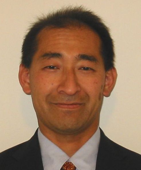
CEO/CTO
Tadao Hashimoto, Ph.D., MBA
Tadao Hashimoto joined Professor Matsunami's laboratory
at Kyoto University in 1990.
His research covered plasma-assisted chemical vapor deposition
(CVD) of amorphous silicon carbide for solar cells and
photo-assisted metalorganic molecular beam epitaxy (MOMBE)
of gallium phosphide. He was awarded bachelor of electrical
engineering in 1991 and master of electrical engineering in 1993
from Kyoto University.
In 1993, he joined Panasonic and worked for 6 years
as a research engineer of semiconductor lasers and
metal organic chemical vapor deposition (MOCVD)
of GaAs-based alloys and GaN-based alloys.
From 1997 to 1999, he stayed at Stanford University as
a visiting researcher working on hydride vapor
phase epitaxy (HVPE) of GaN. In 1999 he left Panasonic and
in 2000 he started his Ph.D study at the University of California,
Santa Barbara. He joined the ERATO Nakamura Inhomogeneous
Crystal Project and started research on the ammonothermal
growth of GaN. In 2005, he was awarded Ph.D in materials
science from UCSB and continued his research on the ammonothermal
growth at UCSB. In 2007, he received Outstanding
Research Achievement Award form Solid State Lighting and Display
Center at UCSB. He is the founder of SixPoint Materials, Inc.
He also completed an online MBA at University of Nebraska, Lincoln
in 2020 with the emphasis of international business.
|
|
Vice President in Technology
Edward Letts, Ph.D
Edward Letts joined Professor Pierre Petroff's laboratory
in UCSB as an undergraduate from 1997-2001. He studied InAs quantum
dot layers grown on GaAs using molecular beam epitaxy.
In 2001 he graduated with honors and was awarded a bachelor
of Physics from the College of Creative Studies at UCSB.
Later that year he started his Ph.D. study at UCSB under
the guidance of Professor Shuji Nakamura.
He researched the bulk crystal growth of AlN using
a sublimation technique. In 2007 he was awarded his Ph.D
in material science from UCSB.
He is the cofounder SixPoint Materials.
|

|